Diffraction gratings are widely used in fields such as precision measurement, laser pulse compression, and spectral analysis. As a maskless lithography method, interference lithography offers high efficiency and flexibility in the fabrication of diffraction gratings. However, the grating size achievable through interference lithography is inherently limited by the aperture of the exposure system’s optical beams, and increasing the aperture of optical elements in the system presents practical challenges. To address this issue, an optical exposure stitching method has been proposed, which expands the grating scale by sequentially shifting and stitching single-exposure regions. The implementation of exposure stitching requires stable and precise global alignment based on external references. The use of reference gratings provides a high-precision and robust alignment method. However, in the field of reference grating-based exposure stitching, no existing approach achieves global alignment in two orthogonal directions on a planar surface.
To meet this demand, Li Xinghui’s group from Tsinghua Shenzhen International Graduate School (Tsinghua SIGS) has proposed an interference lithography stitching exposure method and system based on global alignment using reference gratings. This work provides insights and references for aperture expansion in the fabrication of diffraction gratings.
The stitching exposure system constructed in this study is shown in Fig. 1(a), where the exposure region is generated by two-beam interference, as illustrated in Fig. 1(b). During the stitching process, it is essential to ensure the continuity of fringes across different exposure regions on the substrate, and alignment errors should be monitored in real time during exposure.
The stitching method proposed in this study utilizes two reference gratings to monitor alignment errors in the x and y directions, enabling the expansion of the exposed area across the entire plane. When the two exposure beams are diffracted by the reference gratings, the diffracted beams interfere to produce reference fringes. Any alignment errors are amplified to a macroscopic scale and reflected in the reference fringes, allowing for error compensation based on the obtained error information.
Two reference gratings are employed in this system: one is separate from the substrate, while the other is attached to the substrate and moves along with it. When changing the position of the exposure region on the substrate, one direction is adjusted by shifting the beam position, as shown in Fig. 1(c), while the other direction is controlled by moving the substrate, as illustrated in Fig. 1(d).
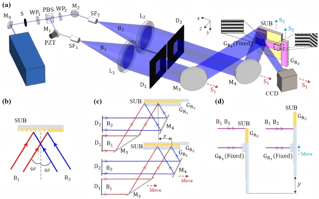
Fig. 1: Grating pattern array exposure system
The stitching exposure process is illustrated in Fig. 2. When stitching within the same row, fringe locking is performed using the reference fringes generated by reference grating GR1, as shown in Fig. 2(a)-(c). In this step, the exposure region position is adjusted by moving a mirror.
For row-to-row stitching, the reference fringes generated by reference grating GR2 must first be locked. Subsequently, the initial reference fringes of GR1 are re-recorded, as shown in Fig. 2(d)-(e). In this case, the exposure region position is adjusted by moving the substrate.
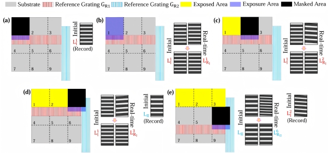
Fig. 2: Fabrication procedure
A 3×3 grating array fabrication was conducted based on the aforementioned system and fabrication procedure. Two sample fabrication experiments were carried out for comparison, with Sample 1 and Sample 2 shown in Fig. 3(a) and Fig. 3(f), respectively. In the fabrication of Sample 1, alignment errors were compensated, whereas for Sample 2, no alignment error compensation was applied.
The diffraction wavefronts were measured using a Fizeau interferometer, and the resulting interference fringe patterns are shown in Fig. 3(b) and Fig. 3(g). The interference fringes of Sample 1 exhibit good continuity across the entire area, while Sample 2 shows noticeable discontinuities in multiple regions. Fig. 3(c) and Fig. 3(h) present the -1st order diffraction wavefronts, while Fig. 3(d) and Fig. 3(i) display the non-flatness of the substrate. After removing the substrate effect, the final diffraction wavefronts are shown in Fig. 3(e) and Fig. 3(j). For Sample 1, the peak-to-valley (PV) value is 0.125λ, and the root-mean-square (RMS) value is 0.023λ. In contrast, Sample 2 exhibits a PV value of 0.621λ and an RMS value of 0.105λ.
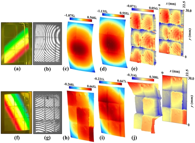
Fig. 3: Fabricated grating arrays
Furthermore, an Atomic Force Microscope (AFM) was used to randomly select a point from each exposure region of the 3×3 area in Sample 1 for AFM measurement. The groove profile is shown in Fig. 4. A low-resolution scan was first performed over a large area, followed by a high-resolution scan over a smaller area. Fig. 5 shows the cross-sectional views of the AFM measurement results, with the groove profiles in each region exhibiting good consistency.

Fig. 4: AFM Measurement Results
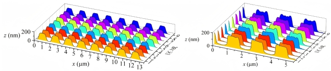
Fig. 5: AFM Cross-Section
To investigate the phase continuity and stitching quality on both sides of the seam, a microscope was used to observe the stitching seam of Sample 1, as shown in Fig. 6. The fabricated fringes in different exposure areas align well with the equidistant and parallel reference lines (red lines), demonstrating their consistent phase, period, and tilt angles. It is important to note that in many applications dominated by surface diffraction, ensuring the consistency of the grating line phase is critical. The control of the physical dimensions of the seam will be further explored in future work.

Fig. 6: Microscope images
The related achievements were recently published in the journal Microsystems & Nanoengineering (Nature publishing group) with the title Global Alignment Reference Strategy for Laser Interference Lithography Pattern Arrays. Associate Professor Li Xinghui is the corresponding author of the paper, and Xiang Gao, a master's student from Tsinghua SIGS, is the first author. Other contributors include Ph.D. student Li Jingwen and master’s student Zhong Zijian, both from Tsinghua SIGS. The project was supported by the National Natural Science Foundation of China and the Shenzhen Stability Support Program.
Research Group Introduction
The research group focuses on the critical objectives of precision and intelligence in advanced manufacturing. Their work spans two main areas: precision measurement technology & instruments and intelligent production technology & equipment. The team has established research directions and platforms in nano-grating interferometric measurement, advanced grating and lithography manufacturing, miniaturized spectrometers and confocal spectroscopy, high-precision and high-dynamic structured light 3D reconstruction, AI-based automatic defect detection, autonomous mobile positioning and navigation, and ultrasonic automated inspection.
Link to full article:
https://www.nature.com/articles/s41378-025-00889-4
Images and written by Xiang Gao & Li Xinghui
Edited by Huang Xiaojia
Reviewed by Nie Xiaomei