Two-dimensional (2D) compound materials are regarded as promising candidates in many applications, such as electronics, optoelectronics, sensors, and flexible devices because they have high carrier mobility, tunable bandgaps, large specific surface area, atomic-level thickness, and other properties.
To bring 2D compound materials from the laboratory to industrial applications, materials preparation is the first step. Among all preparation methods for 2D compound materials, chemical vapor deposition (CVD) is one of the most promising methods as it can grow a series of high quality 2D compound materials at a reasonable cost. However, due to complicated growth mechanisms, maintaining the controllability, repeatability, and high quality of CVD-grown 2D compound materials is still a big challenge and prevents their widespread use.
Recently, a group led by Prof. Hui-Ming Cheng and Associate Prof. Bilu Liu of Tsinghua-Berkeley Shenzhen Institute (TBSI) published a review article titled “Chemical Vapor Deposition Growth of Two-dimensional Compound Materials: Controllability, Material Quality, and Growth Mechanism” in the journal Accounts of Materials Research.
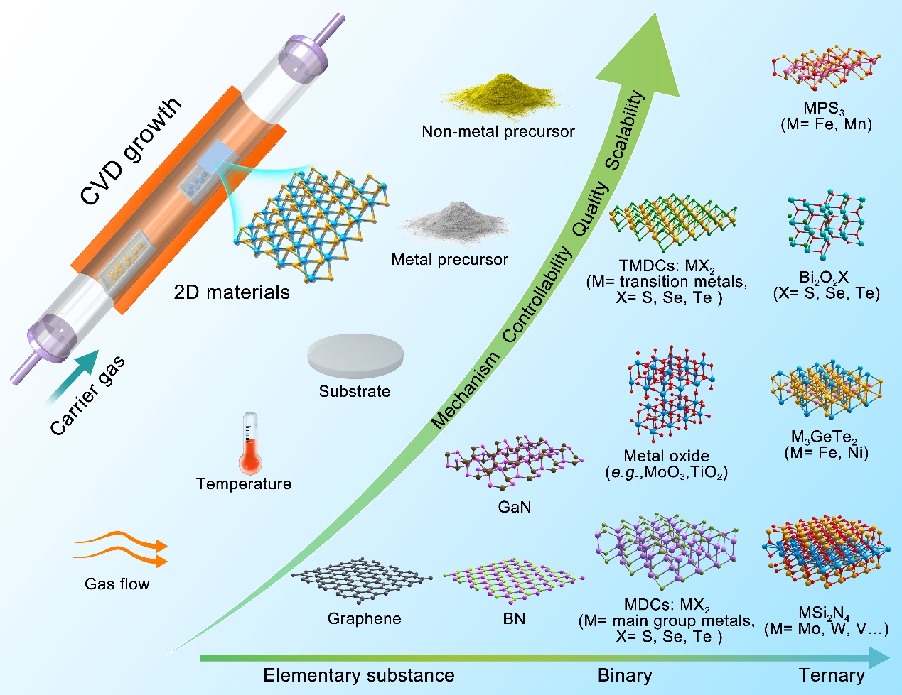
Figure 1. Schematic of the key parameters for CVD growth of 2D materials ranging from elementary substance, binary, ternary to complicated materials
The article reviewed current progress and highlighted promising growth strategies for CVD growth of 2D compound materials. Key technology parameters which affect the CVD process, including non-metal precursor, metal precursor, substrate engineering, temperature, and gas flow, were systematically discussed. The paper also introduced several emerging methods in improving the quality of CVD-grown 2D compound materials (e.g., repairing the sulphur vacancies by thiol chemistry), and summarized current understandings of the CVD growth mechanism. It concluded current challenges and proposed potential opportunities in this field in terms of the growth of novel 2D compound materials (e.g., p-type materials, 2D materials with high carrier mobility, 2D materials with wide bandgaps in the ultraviolet regime or narrow bandgaps in the infrared regime, and 2D non-layered materials), post-treatment of CVD-grown samples to obtain new 2D materials and heterostructures, and the exploration of exotic 2D physics and their promising applications.
This review will serve as a guide for the future design of controllable CVD systems for the growth of high quality 2D compound materials with good controllability, and lay foundations for their potential applications.
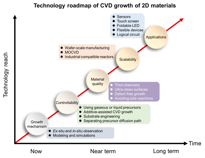
Figure 2. Roadmap of research about CVD growth of 2D materials
The work was supported by the National Natural Science Foundation of China, the National Key R&D Program, Guangdong Innovative and Entrepreneurial Research Team Program, and the Bureau of Industry and Information Technology of Shenzhen.
Link to full article: https://pubs.acs.org/doi/abs/10.1021/accountsmr.0c00063
Editor: Karen Lee
